
C2i Semiconductor tapes out AI power chip, signalling India's advance in chip design
C2i Semiconductor’s tape‑out of an AI‑focused power chip highlights India’s growing prowess in advanced semiconductor design.
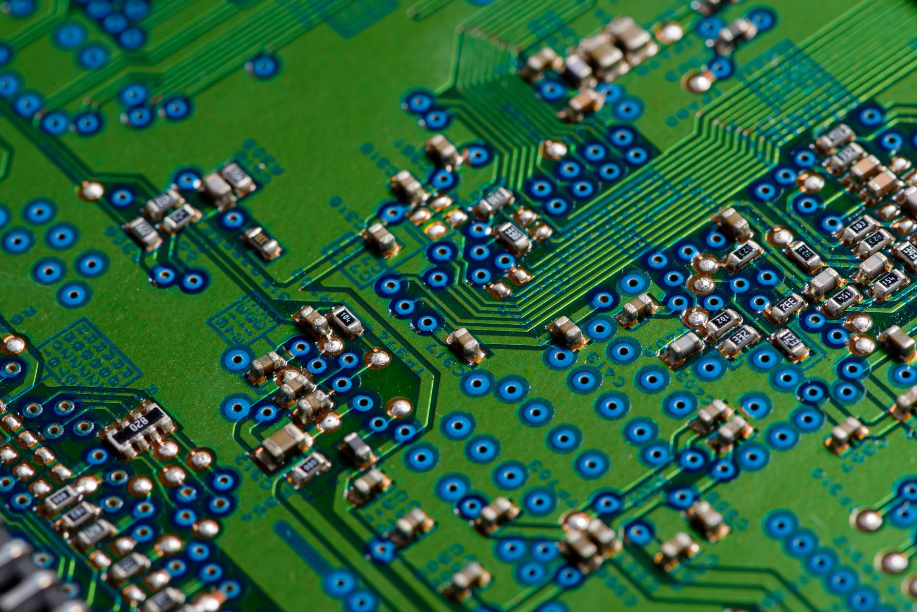
C2i Semiconductor announced that it has successfully completed the tape‑out of its first AI‑power chip, a milestone that the company says signals India’s push into advanced chip design. The tape‑out, which marks the finalization of the chip’s layout before it moves to silicon fabrication, places C2i among a small group of Indian firms capable of delivering complex semiconductor intellectual property for global customers. By targeting the power‑efficiency demands of artificial‑intelligence workloads, the new design aims to sit deeper in the AI infrastructure stack, offering a home‑grown alternative to imported solutions.
What happened
The announcement details that C2i has finished the design phase of an AI‑power chip and handed over the complete layout to a foundry for manufacturing. In semiconductor terminology, a tape‑out is the point at which a design is considered ready for production; it is the culmination of circuit design, verification, timing closure and physical‑design steps. C2i describes the chip as an AI‑focused power solution, meaning it is engineered to deliver high performance while keeping energy consumption low – a critical balance for data‑center accelerators and edge‑device inference engines. The company emphasizes that the tape‑out demonstrates India’s ability to develop sophisticated semiconductor IP that can compete in global markets, rather than merely assembling or testing imported designs.
Why it matters
The tape‑out is more than a technical checkpoint; it signals that India is moving from a reliance on foreign chip designs toward home‑grown, high‑value semiconductor IP. For a country that has traditionally imported most of its AI hardware, the ability to design a power‑efficient AI chip opens pathways to supply‑chain resilience and cost reductions. It also positions Indian firms to capture a share of the rapidly expanding AI hardware market, which analysts estimate will run into hundreds of billions of dollars worldwide. By showcasing a design that can be licensed or integrated into larger systems, C2i potentially creates new revenue streams for Indian tech companies and strengthens the case for further investment in domestic design talent.
The bigger picture
India’s semiconductor ambitions have been formalised through several government initiatives, including the Production‑Linked Incentive (PLI) scheme and the National Semiconductor Mission, both aimed at boosting design, manufacturing and testing capabilities. While most public attention has focused on fab construction, the design ecosystem has lagged behind. C2i’s tape‑out arrives at a moment when Indian startups such as Sanket, Saankhya and others are beginning to file patents for AI‑centric cores, and multinational players are setting up R&D centres in Bengaluru and Hyderabad. The broader trend mirrors a global shift where AI workloads drive demand for specialised power‑efficient chips, prompting countries like the United States, Taiwan and South Korea to double‑down on advanced design. India’s entry into this space, signalled by C2i’s milestone, suggests the nation is attempting to climb the semiconductor value chain rather than remain a downstream assembler.
What’s next
The next logical step for C2i is silicon validation – testing the fabricated chips to confirm they meet performance and power targets. Successful silicon will likely lead to pilot production runs for early customers, possibly in Indian data‑center operators or edge‑AI device manufacturers. The company has hinted at plans to expand its IP portfolio, potentially offering configurable AI cores that can be integrated into system‑on‑chip (SoC) solutions. Observers will watch for partnerships with foundries that can deliver the advanced process nodes required for AI workloads, as well as any government grants that may accelerate the design‑to‑silicon pipeline. In the longer term, a proven AI‑power chip could enable Indian firms to license the design internationally, turning India into an exporter of high‑end semiconductor IP.
Key takeaways
- C2i Semiconductor completed the tape‑out of an AI‑power chip, marking a first for an Indian‑based design house.
- The chip targets power‑efficiency for AI workloads, aiming to sit deeper in the AI infrastructure stack.
- The milestone demonstrates India’s growing capability to create complex semiconductor IP for global markets.
- Success could spur further investment in domestic design talent and reduce reliance on imported AI hardware.
- Watch for silicon validation, pilot production and potential licensing deals as the next phase unfolds.
Frequently asked questions
What does a tape‑out mean in semiconductor design?
A tape‑out is the final stage of chip design where the complete layout is sent to a fabrication plant. It indicates that all design, verification and physical‑design work is finished and the chip is ready for silicon manufacturing.
How could C2i’s AI‑power chip affect India’s technology ecosystem?
If the chip meets its performance and power targets, it could provide Indian companies with a locally designed AI accelerator, reduce dependence on imported hardware, and create export‑able IP that strengthens India’s position in the global semiconductor market.