
Huawei bets on speed over shrinking transistors to sidestep US chip sanctions
Huawei pivots to faster architectures as U.S. bans keep it from the latest EUV lithography tools.
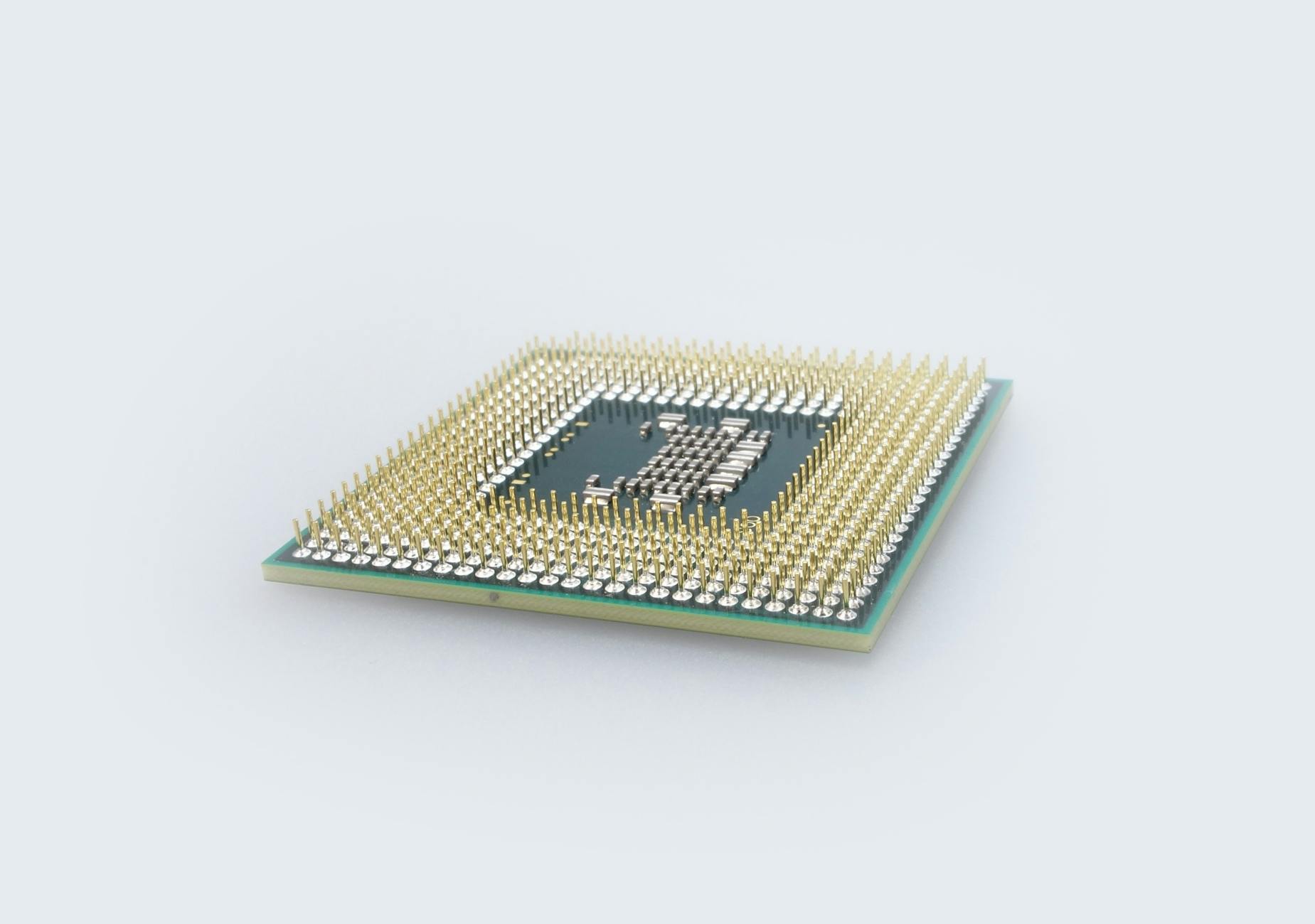
Huawei is shifting its chip strategy toward higher clock speeds and architectural efficiency rather than chasing ever‑smaller transistor geometries, a move designed to work around the United States’ export restrictions that have barred the company from accessing the most advanced lithography equipment since 2019. The Chinese tech giant announced that its next generation of processors will rely on speed‑focused designs, aiming to keep performance competitive while the nation remains cut off from ASML’s extreme ultraviolet (EUV) machines. By emphasizing architectural gains, Huawei hopes to maintain a foothold in high‑end smartphones and data‑center products despite a supply chain that can no longer follow the Moore‑law scaling curve that dominates the rest of the industry.
What happened
Huawei’s leadership outlined a clear technical pivot in a recent analysis published by industry observers. The company is no longer betting on the traditional path of shrinking transistors to achieve performance gains, a path that requires EUV lithography machines that have been off‑limits to Chinese chipmakers since a 2019 ban. Instead, Huawei is investing in design techniques that extract more speed from existing node sizes, such as refined micro‑architectures, higher clock frequencies, and improved power‑efficiency algorithms. The shift is being framed as a practical response to the inability to source the most advanced manufacturing tools, rather than a strategic preference. Sources note that the approach mirrors a broader industry trend where firms compensate for node stagnation with architecture‑level innovation, but Huawei’s case is forced by external sanctions rather than pure market choice.
Why it matters
The decision has immediate implications for Huawei’s product roadmap and for the competitive dynamics of the global chip market. By prioritising speed over node scaling, Huawei can continue to ship devices that meet consumer expectations for performance without waiting for a breakthrough in equipment access. This also signals to U.S. policymakers that sanctions alone may not cripple a determined firm; alternative engineering pathways can sustain a baseline of competitiveness. For rivals such as Taiwan’s TSMC, which still enjoys unfettered EUV access, the move could compress the performance gap in certain segments, especially where raw clock speed matters more than density. Moreover, the shift underscores the growing importance of design expertise and software‑driven optimisation in an era where physical scaling faces diminishing returns.
The bigger picture
Huawei’s strategy reflects a broader recalibration across the semiconductor sector, particularly in markets that face export controls or supply‑chain disruptions. In India, for example, domestic chip initiatives are also exploring architecture‑centric improvements to offset limited access to cutting‑edge fabs. Companies like Tata‑Elxsi and Saankhya are betting on customised IP blocks and AI‑accelerated cores to deliver performance gains without relying on the smallest process nodes. Globally, the same tension is visible at AMD and Intel, which have announced plans to extract more performance from 7nm and 10nm processes through chiplet designs and advanced packaging. Huawei’s pivot therefore aligns with a growing recognition that transistor shrinkage is no longer the sole lever for progress, especially when geopolitical factors restrict tool availability.
What's next
Analysts expect Huawei to roll out a new line of processors within the next 12‑18 months that showcase the speed‑first philosophy. Watch for announcements around its Kirin or Mate series smartphones, where higher clock rates could be highlighted as a selling point. The company is also likely to deepen collaborations with domestic foundries such as SMIC, seeking to optimise existing process nodes for the new architectural targets. In the longer term, any relaxation of U.S. export controls could reopen the EUV pathway, prompting Huawei to revisit node scaling once more. Until then, the firm’s R&D budget will probably stay heavily weighted toward architecture, verification tools, and software stacks that can unlock performance without smaller geometries.
Key takeaways
- Huawei is abandoning the race to shrink transistors, focusing instead on faster, more efficient architectures.
- The shift is a direct response to U.S. sanctions that have blocked access to ASML’s EUV lithography machines since 2019.
- By leveraging design‑level improvements, Huawei aims to stay competitive with leaders like TSMC despite a constrained supply chain.
- The move mirrors a global trend where firms seek performance gains through architecture and packaging rather than pure node scaling.
- Future product launches will likely showcase higher clock speeds as the headline feature, while continued partnership with domestic fabs remains critical.
Frequently asked questions
Why is Huawei focusing on speed instead of smaller transistors?
Because U.S. sanctions have prevented Huawei from accessing ASML’s EUV lithography machines since 2019, making it difficult to produce chips on the latest, smallest nodes. Speed‑focused architectural improvements allow the company to maintain performance without relying on further transistor shrinkage.
How does the EUV ban affect Huawei's competitiveness?
The ban limits Huawei’s ability to use the most advanced manufacturing processes, which could widen the gap with leaders like TSMC. By optimizing design and clock speed, Huawei aims to narrow that gap and continue delivering high‑performance products.